
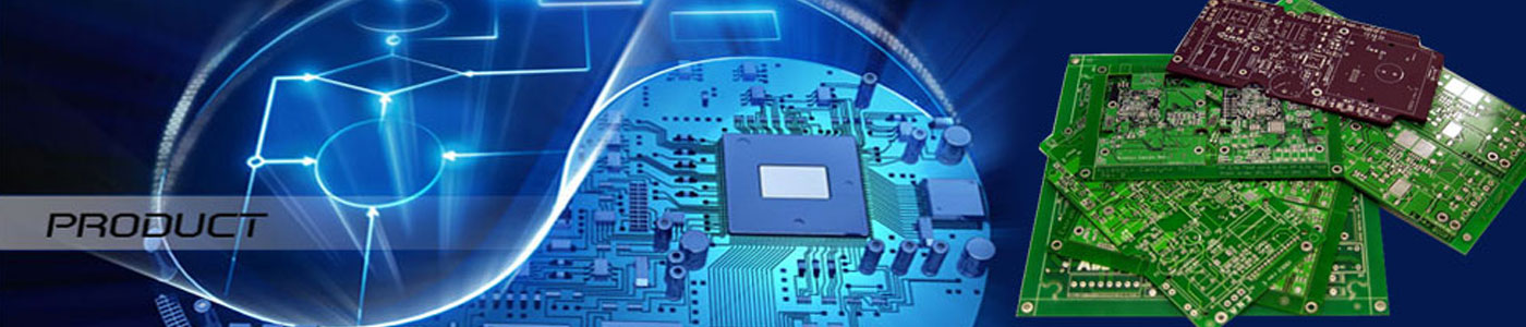
Welcome To PCB Informatics
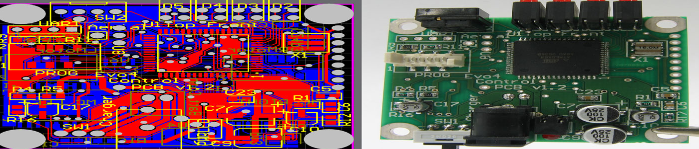
PCB Informatics offers High Speed PCB Design Services, Component Library Creation and Signal Integrity Analysis with Quality On-time deliverables. We have expertise in high speed PCB design in the area of Computing, Networking, Telecom, Consumer electronics and we also expertise in Power supply, and Probe card PCB design. We have design knowledge in all the high speed interfaces like DDR II, DDR III, QDR, FSB, SDRAM, PCI, PCI-X, PCI-E, SATA, USB, HDMI, SDIO, SPI and LVDS.
Our Layout Engineers are IPC Certified Interconnect Designers and are members of the IPC Designers Council.
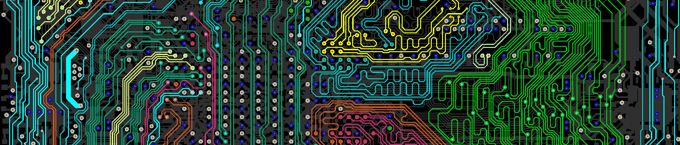
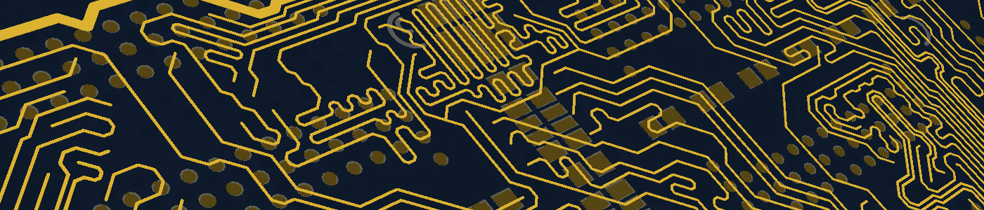
• Multi-Layer, Single-Layer, Double-Sided, Blind and Buried Vias.
• Fine line, Curved Traces, Teardrop Pad Generation, Copper Pour and Split / Mixed Planes.
• High-Speed, Matched Impedance and Differential Pairs.
• Analog, Digital, High Voltage and High Current.
• Gate Swap, Pin Swap, Forward and Back ECOs.
• Rename Reference Designators and Back Annotate Schematics.
• Comprehensive checklists, Layout Guidelines and DRCs.
• Schematic Capture and BOM generation.
PCB Informatics maintains an extensive library of standard components and has developed a unique
naming convention that is easy to follow and understand. Libraries contain the part
designator, manufacturer data, specific attributes and PCB decal, which makes specific or
custom BOMs easy to generate.